Magnetization reversal in triangular microstructures

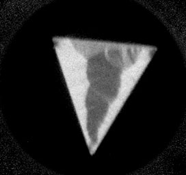
   The image shows the domain pattern in a lithographically patterned polycrystalline Co triangular microstructure of 30 nm thickness on silicon. The magnetization reversal behavior of such microstructures can be followed with the PEEM by applying short magnetic field pulses between the acquisition of domain images.

   White contrast means the magnetization vector is pointing towards the top of the image, dark contrast means it is pointing towards the bottom. Intermediate grayscales indicate horizontal magnetization directions. Field of view: 55 μm.

   See a QuickTime Movie (300 kB) of the magnetization reversal of these triangular microstructures (needs QuickTime Player).

   These studies were performed at SPring-8 in Japan in collaboration with S. Imada and S. Suga, Osaka University.

   Publication: Japanese Journal of Applied Physics 39, L585 (2000).


   Magnetization reversal in an array of ultrathin Co microstructures

   Arrays of Co microstructures as thin as 6 atomic layers (=1 nm) were prepared on a Cu(001) single crystal substrate by evaporation through a gold mesh with 25.4 μm period. A large field of view of the PEEM was selected in order to study the magnetization switching of many squares ("survey mode", =0.3 mm field of view).

   The figure shows a PEEM image of an array of ultrathin Co squares on Cu(001). Bright squares have already switched their magnetization direction in external magnetic field pulses. The dark squares exhibit a higher coercivity, which is probably determined by a macroscopic morphological peculiarity of the substrate. Field of view: 300 μm.

   Consecutive images after the application of short magnetic field pulses of increasing strength Download the movie of magnetization reversal in these microstructures (QuickTime Movie, 2 MB). (To play the movie, QuickTime Player is needed).

   These studies were performed at SPring-8 in Japan in collaboration with S. Imada and S. Suga, Osaka University.


back to "Magnetic imaging by photoelectron emission microscopy"